Someone asked me the other day: “What actually happens inside a PCBA factory? Like, step by step?”
I get that question a lot. Most people think you just send a design file and magic happens. The reality is messier, louder, and way more interesting.
So here’s a real, no‑BS walkthrough of how a bare PCB turns into a working PCBA. No textbook language. Just what happens on the factory floor.
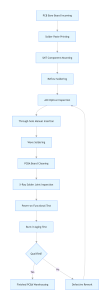
Step 1: They Put Goo on the Board (Solder Paste)
Yeah, “goo” is the technical term. It’s actually solder paste – tiny balls of metal mixed with flux. Looks like gray play‑doh.
A machine presses this goo through a stencil (a thin metal sheet with holes exactly where your pads are). The paste sticks to the board.
What can go wrong?
Too much goo → shorts. Too little → no connection. Stencil misaligned → paste on the wrong spots.
Good factories check this with a fancy camera machine (SPI). Cheap factories just eyeball it and hope for the best. If you want reliable boards, ask your CM: “Do you have SPI?” If they say no, think twice.
Step 2: Robots Place Tiny Parts (Pick & Place)
This is the satisfying part. A machine with little nozzles picks up resistors, capacitors, chips – some smaller than a grain of sand – and plops them onto the sticky paste.
It’s like a really expensive, super‑accurate version of playing “Operation.”
The machine follows a file from your PCB design. If your design has bad fiducial marks (those little copper dots that help the robot see where to place), the parts end up crooked. Then you get tombstoning later – where a tiny part stands up like a gravestone because it soldered wrong.
I’ve seen it happen on a customer’s board. They blamed the factory, but we pulled up the design file and… yeah, the fiducials were missing. Oops.
Step 3: Into the Oven (Reflow Soldering)
Now the board goes through a long oven – like a pizza oven but longer and way more precise.
Temperature goes up slowly, melts the solder paste, then cools down. The parts get soldered permanently.
True story from a friend’s project
He had a batch of boards where every single one had cracked ceramic capacitors. Spent two weeks blaming the component supplier. Turned out the reflow oven had a broken temperature sensor and was heating up too fast. The factory didn’t catch it because they didn’t run a proper “profile” for his board.
Now he always asks for a copy of the reflow profile. Most people don’t. But that one lesson saved him thousands later.
Step 4: Big Parts Get Pushed Through Holes (Through‑Hole)
Not everything can be placed by a robot. Connectors, big capacitors, switches – they have legs that go through holes in the PCB.
Someone (or a machine) inserts them manually. Then the pins stick out the bottom, waiting to be soldered.
This step feels old‑school. But for big parts, it’s still the best way.
What annoys me
Some designers forget about through‑hole parts until the last minute. Then they realize the board has to be flipped, or the parts are too tall for the case. Check your mechanical clearances early – or you’ll be that person.
Step 5: Wave Soldering – Like a Tiny Tsunami of Metal
For those through‑hole pins, the board passes over a flowing wave of molten solder. The wave touches the bottom side and solders all the pins at once.
It’s kind of beautiful to watch. Also terrifying if you think about it too much.
But here’s the catch: if you have surface‑mount parts on the bottom side, they’ll get drowned in solder. So you either mask them or use “selective soldering” – a robot that goes only to the through‑hole pins.
Selective soldering is slower. Your factory will charge more. But sometimes there’s no way around it.
Step 6: Do They Clean It? (Ask This Question)
Modern solder paste is “no‑clean,” which means the leftover flux is supposedly harmless. So most factories skip cleaning entirely.
But here’s the real talk: “no‑clean” doesn’t mean clean. For high‑impedance circuits, medical devices, or anything RF, that leftover flux can cause leakage currents and weird failures months later.
I know a guy who made a humidity sensor board. Worked perfectly in the factory. Failed in the field after a few weeks. The cause? Flux residue absorbing moisture.
Now he always asks: “Do you clean boards as standard? If not, what’s the extra cost?” Sometimes it’s worth it. Sometimes it’s not. But at least you know.
Step 7: Testing – Where Dreams Come True or Die
This is the step you cannot skip. Ever.
Three common ways to test:
AOI (Automated Optical Inspection) – Cameras look at the board. Fast. Good for catching missing parts or obvious bad joints. But it can’t see inside a BGA chip.
ICT (In‑Circuit Test) – A bed‑of‑nails fixture touches test points and measures resistors, capacitors, shorts, opens. Very reliable. But you need a custom fixture, which costs money and takes time.
FCT (Functional Test) – You power up the board and run actual firmware. Push buttons, blink LEDs, read sensors. This is the real proof.
Honest advice from years of watching this
For prototypes: just do FCT.
For production: ICT + FCT if you can afford it.
For cheap stuff: AOI only – but be ready for some field failures.
Step 8: Coating – If Your Board Lives in a Rough World
If your product will see humidity, dust, salt, or chemicals, you need conformal coating – a thin plastic layer sprayed over the board.
It protects against the elements. But it makes rework a nightmare. Once coated, you can’t just swap a part easily.
Real example
A customer made a controller for an outdoor pool pump. No coating. After one season, corrosion killed half of them. The next batch with coating? Still running after three years.
So if your product goes outside, in a kitchen, or anywhere near moisture – coat it. If it sits in a dry, clean living room, skip it.
What Happens After All This?
The factory cuts the panel into single boards (if they were made as one big panel), does a final visual check, and packs them.
Then they ship. Then you wait. Then you finally hold a working board and feel like a genius.
Until you realize you forgot to add a test point for something. But that’s a story for another blog.
A Few Things I’ve Learned (Sometimes the Hard Way)
The cheapest assembly quote is rarely the cheapest in the long run.
Low price usually means skipping steps – no SPI, no cleaning, minimal testing. You’ll pay for it in rework and returns.
Your design mistakes become their production nightmares.
If you don’t leave enough space between components, the pick‑and‑place machine can’t place them without collisions. Seen it. Done it. It hurts.
Build a relationship with your CM’s process engineer.
Buy them coffee. Ask dumb questions. They’ll save you from yourself.
Always, always get a DFM review before they start.
If your factory doesn’t offer DFM, find another factory.
That’s It, Really
PCBA assembly isn’t magic. It’s a bunch of machines and people doing a bunch of small steps perfectly, over and over. When it works, you don’t think about it. When it fails, you think about nothing else.
Now you know what happens inside that factory. Next time you get a quote, you can ask smarter questions – like “Do you have SPI?” and “What’s your typical reflow profile?” and “Can you send me a DFM report?”
They’ll know you’ve been around. And that’s a good thing.
